10 Tips for Successfully Implementing EMC Testing in the Automotive Industry
 Data:2022-09-21
 Click:2879


Data:2022-09-21
Click:2879
Preface
The automobile industry and every automobile enterprise must meet various electromagnetic compatibility (EMC) regulations and EMC tests. For example, there are two requirements to ensure that the electronic system does not cause too much interference signal (EMI) or noise. It must be able to avoid the noise generated by other software. This paper studies some such regulations and discusses some techniques and methods to ensure that the equipment design meets these requirements.
Brief description of EMC regulations
CISPR25 is a specification that provides several test standards with recommended limits to evaluate the radiation transmission formed by components to be installed on the vehicle. In addition to providing guidance for manufacturers, most manufacturers also have their own set of standard CISPR25 supplementary guidance rules. The purpose of CISPR25 test is to ensure that the components installed in the vehicle will not affect other software in the vehicle.
CISPR25 stipulates that the electromagnetic noise level in the test room must be at least 66dB lower than the minimum electrical frequency. Because the desired noise level of CISPR25 is as low as 18dB( μ V/m), so a place less than 12 dB is required( μ V/m) ambient noise level. As a reference, this is roughly equivalent to the broadcast field strength of a typical AM radio station with a distance of 1 km from the antenna.
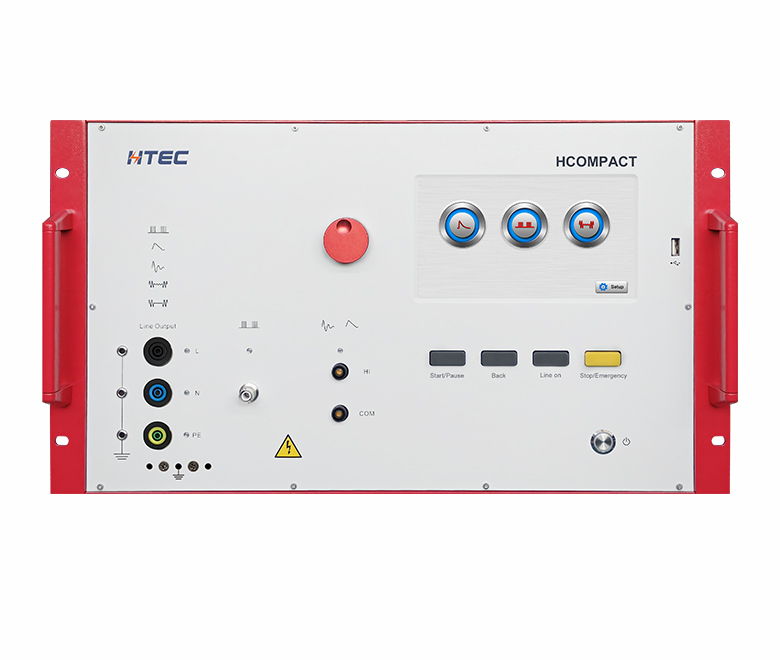
In today's environment, the only way to meet this requirement is to test in a unique room designed to shield the test environment and external magnetic field. In addition, because the normal budget needs to limit the size of the detection room, it is very important to avoid the adverse impact of signal reflection in the detection environment of the detection room. Therefore, the wall of the test room must be embedded with a material that does not reflect electromagnetic (EM) waves (Figure 1). The cost of the testing room is very expensive, and it is usually rented every hour. In order to reduce costs, it is best to correctly evaluate the EMC/EMI problems in the design, and then complete a success in the testing room.
1、 Keep small loop
When there is a magnetic field, the loop formed by conductive material acts as an antenna and converts the magnetic field into current flowing around the loop. The current intensity is positively correlated with the area of the closed loop. Therefore, the presence of loops should be prevented as much as possible and the area of necessary enclosed areas should be as small as possible. For example, when there is a differential data signal, there may be a loop. A loop is formed between the transmitter and receiver that select the differential line.
Another common circuit occurs where the two subsystems use the same circuit, perhaps a display and a module control circuit to push the display (ECU). There is a common ground (GND) line in the chassis and a connecting line from the overall ECU end to the GND. When the video signal is connected to the display screen with its own ground wire, it will form a huge loop in the ground plane. In some places, this kind of circuit is inevitable. However, despite the introduction of inductance or ferrite beads in the ground connection line, the DC loop will still exist, but from the perspective of RF radiation, this loop has been broken.
In addition, each pair of differential controllers/receivers will also form a loop when transmitting signals according to twisted pair cables. Generally speaking, because the twisted pair is tightly connected, the loop area of the connecting cable part is very small. However, once the signal reaches the circuit board, it should be kept tightly connected to prevent expansion of the circuit area.
2、 Bypass capacitance is indispensable
CMOS circuits are very popular, partly because of their high speed and very low power. When CMOS needs to be charged and discharged, the circuit only consumes power when it changes and node capacitance. From the perspective of power supply, CMOS with an average flow consumption of 10mA may absorb many times more current during clock conversion, but the flow consumption during clock conversion is very low or even zero. Therefore, the radiation limitation method focuses on the peak value of voltage and current rather than the average value.
In the clock conversion process, the current surge from the power supply to the chip power supply pin is the main radiation source. According to the bypass capacitor around each power pin, the capacitor will directly provide the current needed to power the chip during the clock pulse edge. Then, in the middle of the clock conversion cycle, the charge in the capacitor uses a low and stable current accumulation. Larger capacitors are suitable for current surges, but their response to fast standards is poor. In particular, small capacitors can quickly respond to demand, but their total charge capacity is limited and consumption is fast. For most circuits, the best solution is to mix capacitors of different sizes (maybe 1 μ F and 0.01 μ F Capacitors in parallel). The smaller capacitor can be placed in the area very close to the power pin of the device, while the larger capacitor can be placed in the area far away from the power pin.
3、 better matching resistance can minimize EMI
When a fast signal is transmitted according to the transmission line and the characteristic impedance changes on the transmission line, part of the signal will be reflected back to the signal source, and part of the signal will continue to transmit along the original direction. Reflection will lead to radiation, which is always the same. To achieve low level EMI, appropriate rapid design practices must be followed. There are a lot of excellent resources to bring you relevant customized transmission line information. The following are some precautions proposed when designing transmission lines:
Remember that there is a signal between the ground plane and the signal wiring. Radiation may be caused by the final disconnection of the ground plane of the signal wiring, so pay attention to the trauma or final disconnection of the ground plane under the signal wiring. Try to avoid obtuse angle in the arrangement of signal wiring. Exquisite corners are much better than right angles.
Generally, FPD-Link signal will allow parts to tap it; For example: coaxial power supply, power connection, AC lotus capacitor, etc. In order to minimize the reflection in the assembly, you can try to apply the widget of 0402 model and set the wiring width to the same width as the welding layer of 0402 assembly. In addition, the characteristic impedance of the wiring shall be set according to the thickness of the dielectric in the operating layer.
4、 Shielding
We should use good shielding methods. There is no shortcut to this point. When the design is designed to minimize radiation, shielding is required around the part that causes the problem circuit. Although it can still radiate energy, better shielding can capture radiation and send it to the ground before they escape the system. The figure below shows how to manipulate the shielded EMI.

Shielding can be used in various forms. It may be easy to shut down the system in a conductive shell, or it may be a small customized plastic shell welded above the radiation source.
5、 Short ground wire
All current injected into the chip will also be discharged from the chip again. Several methods introduced in this paper mention that the connection line of the chip must be short, for example, the bypass capacitor should be close to the IC and maintain a small circuit. However, when the grounding current returns to its origin, the path that must be passed is often abandoned. Ideally, one layer of the circuit board is dedicated to grounding until the GND path is no longer than a through hole. However, some circuit boards have a wound on the ground plane, which drives the ground current from the chip back to the power supply. GND When current is transmitted in this way, it acts as an antenna to push or receive noise.
6、 The rate shall not exceed the required level
There is a trend in the industry to worry about timing margin and use the fastest possible logic device to give the best time margin. Unfortunately, very fast logic devices have steep pulse edges and very high frequency components, which will generate EMI. One measurement method to reduce system EMI is to use logic devices with the lowest possible rate but still reaching the time standard. FPGA allows the drive strength to be set at a lower level, which is a way to reduce the edge speed. In some places, the series resistance on the logic line can be used to reduce the signal conversion rate in the system.
7、 Power line inductance
In the second method, we discuss that the bypass capacitor can be used as a means to reduce the harm of current surge. The inductance in the power line is another level of the same problem. By arranging inductance or ferrite beads on the power line, the circuit that is forced to connect to the power supply can meet the dynamic power requirements of the capacitor (not the power supply).
8、 The capacitor is arranged at the input end of the switching power supply
What car designers worry about is the AM electromagnetic band. Most cars are equipped with an AM recorder with a very sensitive high-gain amplifier with a tunable frequency range of 500kHz to 1.5MHz. If a component sends a signal in this frequency band, it is likely that AM I heard in the recorder. Many switching power supplies use switching frequencies within this frequency band, which leads to problems in automotive applications. Therefore, the switching frequency of most automotive switching power supplies is higher than this frequency band - usually 2MHz or higher. If sufficient filtering is not provided at the input or output end of the switching power supply, this switching noise will enter other subsystems sensitive to the fundamental frequency or sub-harmonic frequency.
9、 Pay close attention to resonance
For various interference sources, inductors and capacitors need to be used to alleviate the dv/dt and di/dt problems of possible EMI problems. However, inductors and/or capacitors have adverse characteristics that are unrelated to self-resonance. This situation can usually be corrected by increasing the resistance connected to the inductor. This resistance can absorb the kinetic energy generated by vibration, thus avoiding its increase to the extent that it is enough to cause problems. When there is a series inductor leading to a component containing a bypass capacitor (separate component from the power line or parasitic inductance), it will cause another hidden problem. The resulting L-C may oscillate at the resonant frequency. Similarly, this situation can also be solved by resistance (usually in parallel with inductor).
10、 Peak radiation can be reduced by spread spectrum recording
For FPD-Link serializer or deserializer (SerDes), for other components, there is usually a data bus and clock with the spread spectrum timing option. In spread spectrum recording, the clock signal is modulated. As a result, the energy propagation caused by the clock and signal pulse edge is in a wider frequency range than the frequency band that must be occupied. Because the EMI standard is set to limit the peak radiation of all frequencies in a frequency band, spreading noise in a wide frequency band helps to significantly reduce the noise peak. DS90UB914A-Q1 is a good case of string resolver, which is often used with DS90UB913A-Q serializer. This device is used for excellent driving assistance system (ADAS) video link between camera and processor. The decoder undertakes the clock provided by the image sensor in the camera to the serializer, and exports the clock Cpu application with the data. 10 or 12 fast data lines and fast clock simultaneously change control is a major source of EMI. In order to reduce this EMI, the DS90UB914A has the option of applying the spread spectrum clock and exporting data (instead of the low vibration clock provided by the image sensor). The spread spectrum clock is controlled according to the memory in the descaler.
Epilogue
As cars increasingly rely on electronic devices to achieve not only entertainment and comfort, but also entertainment and comfort, it is necessary to achieve error-free operation and the impact of other software. According to the technologies and methods briefly described in this article, and selecting the appropriate components for EMC testing, engineers can design a stable system, so that the vehicle system will not be affected EMI will be affected by the problem, and work reliably.